Hi-Tech Products Die Cutting and Converting

Microfuidic Device Manufacturing

Hi-Tech Products can provide the materials and converting processes necessary to manufacture your microfluidic components. Materials may include converted film, membrane, and foil components commonly found in microfluidic device assembly. Our ISO certified facilities and expertise are well suited for manufacturing: microfluidic chips, PCR chips, flow cells, cartridge consumables, lateral-flow, NGS flow cells, and wearable patches.

Structural & optical films

  • Optical cover / detection window
    • Materials: COC, COP, PC, PMMA, thin glass.
    • Thickness: 50–1000 µm (commonly 100–500 µm).
    • Processes: laser cutting, die-cutting, precision sheeting, ultrasonic welding prep.
    • Use: fluorescence/absorbance readout, microscope optics, alignment windows.
  • Substrate film (bulk structural layer)
    • Materials: COC/COP, PC, PET, PEN.
    • Thickness: 100–2000 µm.
    • Processes: die-cutting, CNC routing (if laminated to rigid support).
    • Use: base layer for channels, mounting reagents, mechanical support.

Adhesive & bonding layers

  • Pressure-sensitive adhesive (PSA) die-cuts / transfer tapes
    • Materials: acrylic PSAs, silicone PSAs, rubber PSAs (medical grade).
    • Thickness: 25–250 µm (1–10 mil).
    • Processes: lamination, kiss-cut, through-cut, transfer coating.
    • Use: seal microfluidic layers, form channels by selective bonding, tack for assembly.
  • Thermoplastic welding films / thermal bond adhesives
    • Materials: polyethylene, polypropylene, specialized thermoplastic films.
    • Thickness: 25–200 µm.
    • Processes: thermal lamination, impulse welding.
    • Use: permanent seals for reaction chambers that require high-temp exposure.
  • Double-sided tape with patterned release liners
    • Use: rapid assembly, pre-registered adhesive patterns to control fluid paths.

Channel-defining & spacer films

  • Patterned spacer adhesives (channel-forming die-cuts)
    • Materials: acrylic adhesive on PET/film carriers, laser-cut PSA.
    • Thickness: 25–500 µm depending on channel depth.
    • Processes: die-cut, laser-cut, plotter cutting.
    • Use: define channel geometry, create reaction chamber volumes.
  • Embossable thermoplastic films for molded channels
    • Materials: COC, COP, PC.
    • Processes: embossing, hot-emboss die forming.
    • Use: formed microchannels for precise fluid handling.

Membranes for filtration, venting, and metering

  • Hydrophobic vent membranes (air venting / bubble trap)
    • Materials: PTFE, ePTFE, PVDF with hydrophobic treatment.
    • Pore sizes: 0.1–5 µm (application dependent).
    • Processes: die-cut, adhesive-backed options.
    • Use: allow air escape while blocking liquid; pressure relief vents.
  • Hydrophilic membranes (wicking / flow control / capillary stop)
    • Materials: nitrocellulose (lateral flow), cellulose, polyethersulfone (PES), hydrophilized PTFE.
    • Pore sizes: 0.1–10 µm.
    • Processes: precision die-cutting, overlamination.
    • Use: capillary flow, reagent distribution, filtration.
  • Filtration membranes (particle/virus filtering)
    • Materials: PES, PVDF, cellulose acetate, nylon.
    • Pore sizes: 0.02–5 µm.
    • Use: remove particulates, pre-filter sample.
  • Porous foam membranes (wicking / absorbent pads)
    • Materials: PU foam, cellulose foam.
    • Use: waste reservoirs, absorb excess reagent.

Valve, burst, and metering films

  • Pressure-actuated valve membranes
    • Materials: thin elastomers (TPU, PDMS), laminated films with cutouts.
    • Thickness: 25–200 µm.
    • Use: on-chip valves that open/close with pressure or vacuum.
  • Burstable foil / peel-seal membranes (reagent isolation)
    • Materials: aluminum foil laminates, metallized PET, multi-layer foil.
    • Processes: die-cut, heat-seal, laser scoring.
    • Use: isolate lyophilized reagents or reagents until use; scored weak points for controlled rupture.
  • Capillary burst valves (hydrophobic patches on film)
    • Materials: surface-treated PET/COC with hydrophobic coatings or patterned adhesives.
    • Use: passive flow control via capillary pressure thresholds.

Reagent & storage films / seals

  • Foil laminate seals (moisture/oxygen barrier)
    • Materials: Al foil laminated with PET/LDPE; multi-layer barrier films.
    • Processes: form-fill-seal, die-cut seals.
    • Use: reagent pouch covers, lyophilized reagent pouches, long-term storage.
  • Desiccant films / sachet foils
    • Materials: laminated foil pouches, breathable desiccant-embedded films.
    • Use: maintain dry environment for reagents.
  • Transfer/spotting carriers for dried reagents (paper/film backing)
    • Materials: glass fiber pads, porous membranes laminated to film.
    • Use: hold lyophilized enzymes, primers, probes inside chamber.
    •  

Conductive & thermal films

  • Printed conductive traces / thin-film heaters
    • Materials: silver/graphene/sputtered metal traces on polyimide, PET, or COC.
    • Processes: screen print, inkjet, sputter, flex circuit lamination.
    • Use: on-chip heaters for PCR thermal cycling, temperature sensors, electrical contacts.
  • Flexible printed circuit interposers (polyimide flex)
    • Materials: polyimide with copper traces, laminated to PET.
    • Use: connect chip electrodes to instrument, sense signals, apply voltage.
  • Thermal interface films / heat-spreading foils
    • Materials: graphite films, thin metal foils.
    • Use: even heat distribution across reaction chambers.

Optical control & stray-light management

  • Black/opaque films
    • Materials: black PET, black COC, carbon-loaded films.
    • Use: prevent optical cross-talk between wells and block stray light.
  • Reflective films / metallized foils
    • Materials: aluminized PET.
    • Use: increase signal by reflecting excitation/emission.
  • Anti-reflective / anti-glare coatings on detection windows
    • Processes: coatings applied to films for better optical performance.

Surface-treated films & coatings

  • Hydrophilic surface treatments (promote wetting)
    • Methods: plasma, corona, chemical grafting, surfactant coatings.
    • Use: control capillary flow, reduce air bubbles.
  • Hydrophobic coatings / patterning
    • Use: capillary stops, channel definition.
  • Anti-fouling / PEG coatings
    • Use: reduce nonspecific protein/DNA adsorption, improve assay sensitivity.
  • Adhesion promotion layers
    • Use: improve bonding between dissimilar plastics or adhesives.

Release liners & handling carriers

  • Silicone-coated release liners (paper or film-backed)
    • Use: protect PSA until assembly, register die-cuts for pick-and-place.
  • Low-tack carrier films (transfer tapes)
    • Use: temporary support of fragile microfluidic components during assembly.
9744-Liner-White-Background

Lidding & user interface films

  • Peelable user-access films
    • Materials: easy-peel laminates, scored foils with tamper-evident features.
    • Use: sample ports, user-accessible reagent chambers.
  • Labeled overlays / instruction films
    • Materials: printable PET/PVC overlays, with tactile features.
    • Use: labeling, user guidance, barcode placement.

Sterilization- & process-compatibility notes

  • Gamma / EtO / E-beam compatibility: specify material compatibility up front (e.g., some PSAs yellow or lose adhesion under gamma).
  • Autoclave: most polymer films warp; use only materials rated for steam if required.
  • Shelf-life & packaging: barrier foils + desiccants often required for lyophilized reagents.

Typical converting processes used

  • Die-cutting & kiss-cutting — precision cut shapes for PSAs, membranes.
  • Laser cutting — tight tolerances, small features, no tooling.
  • Lamination — roll-to-roll or sheet lamination to build stacks.
  • Embossing / hot-emboss — create microchannels in thermoplastics.
  • Printed electronics (screen/inkjet/sputter) — heaters, traces, electrodes.
  • Thermal/ultrasonic/laser welding — permanent seals between thermoplastic layers.
  • Plasma/corona treatment & coating — tuning surface energy.
  • Punching & stamping — high-volume shapes.

Typical tolerances & specs to call out on drawings

  • Channel depth tolerance: ±5–20 µm (depends on process).
  • Die-cut hole positional tolerance: ±0.05–0.25 mm (depending on tool & material).
  • Adhesive placement tolerance: ±0.2 mm typical for high-precision.
  • Surface roughness / optical clarity: specify % haze, transmission.
  • Pore size distribution (membranes): specify mean pore size ± SD.
  • Biocompatibility: USP Class VI / ISO 10993 requirements if in contact with sample or tissue.

Example component→material→use quick mapping (short)

  • PCR optical window → COC, 200 µm → fluorescence read.
  • Channel spacer → PSA on PET, 100 µm die-cut → microchannel definition.
  • Reagent foil seal → Al/PET/LDPE laminate → foil seal over reagent well.
  • Hydrophobic vent → ePTFE membrane, 0.2 µm → air vent.
  • Lyophilized reagent pad → glass-fiber pad laminated to substrate → dried enzyme spot.
  • On-chip heater → printed silver on polyimide → rapid thermal cycling.

Converting Capabilities

Hi-Tech Products is proud to be a 3M / Solventum Premier Converter.

A 3M / Solventum Premier Converter has certified expertise, backed by a history of 3M / Solventum quality and innovation.

Hi-Tech Products understands the industry and exceeds expectations. 3M Preferred Converters have certified expertise, backed by a history of 3M quality and innovation. Count on this shared industry knowledge and experience to enable us to provide the highest quality materials and precision die cutting manufacturing.  See more.

No substitute for experience

Hi-Tech Product’s die cutting specialists deliver high quality die cutting company services. Founded in 1979 by Jim Ruch, a Mechanical Engineer, Hi-Tech Products is one of the most advanced providers of die cutting services in the USA.  Hi-Tech Products is ISO 13485:2016 certified, ISO 9001:2015 certified, and operates multiple locations in the USA and Mexico, to serve our global customers’ converting, assembly, and packaging needs.

rotary die cutting services reliability

Rotary Die Cutting Services Reliablity

Since 1979, Hi-Tech has established a reputation for on-time delivery, quality & consistency. Because of our ongoing level of service, confidentiality, and integrity, the majority of our customers have been with us for over 10 years.

Adhesive Converter California – Hi-Tech Products is based in Buena Park California and performs precision die cutting in certified cleanrooms.

rotary die cutting services experience

Converting Specialists and Industry Experience

With over 40 years in the business of rotary die cutting services and more than 400 active customers, Hi-Tech Products has developed processes that meet the most demanding requirements & specifications.

Hi-Tech has been involved in the development of a wide range of products for virtually every application. This depth of experience & materials knowledge allows Hi-Tech to often provide critical insights to help clients avoid expensive mistakes.

precision die cutting services factory

Die Cut Products Manufacturing

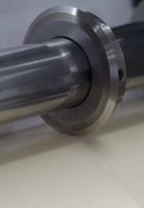
With two facilities in the USA and Mexico, Hi-Tech Products has a wide range of capabilities and provides every type of die cutting service.

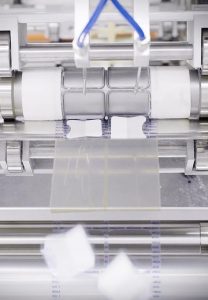
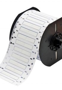
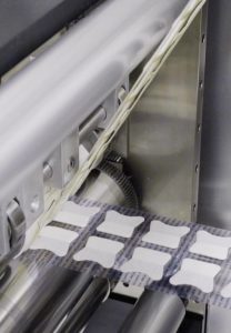
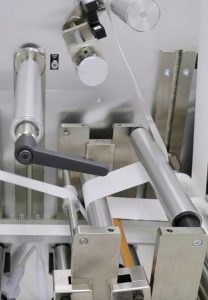
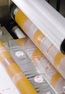
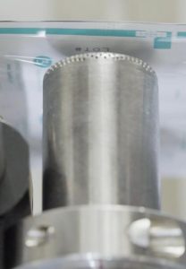
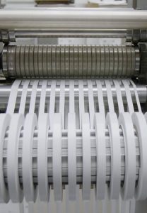
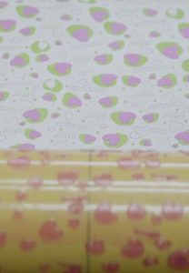
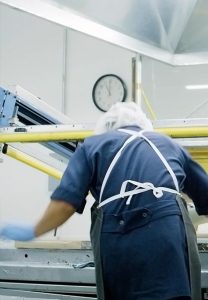
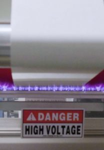
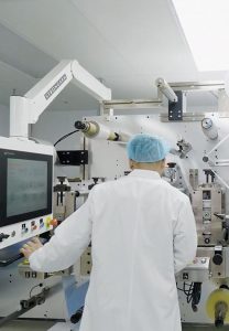
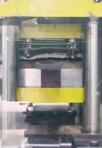
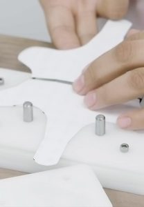
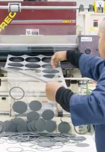
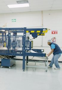
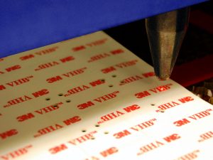
Our converting services include precision die cutting, laminating, slitting, printing, RF welding, and laser can be done in certified cleanrooms. Labor intense converting, packaging, and assembly are performed in Mexico at off-shore labor rates.

Hi-Tech Products is also a CTPAT Partner making importing from our factory in Mexico fast, efficient, and reliable.

CTPAT certified

Die Cutting and Converting Materials Partners